Quantum hardware sounds ethereal. The machining behind it isn’t. It’s brutally concrete: microns of flatness, microinches of roughness, thermal paths that actually conduct at 10 mK, and seals that hold ultra-high vacuum (UHV) for months without drama. When those numbers slip, coherence times, readout fidelity, and uptime slip with them.
This post breaks down the critical tolerances and finishes for common quantum subsystems—and how Ziqual hits them repeatably.
Why Machining for Quantum Is Different
Quantum platforms (superconducting, ion-trap, neutral-atom, photonic) all stack four unforgiving constraints:
- Cryogenics: Metals shrink non-uniformly from 300 K to millikelvin. Joints must still mate perfectly cold.
- Microwave/RF & Optics: Surface roughness and seam quality set loss and parasitics. Slight geometry errors shift resonances.
- Ultra-High Vacuum (UHV): Every burr, smear, and oil residue becomes an outgassing or leak risk.
- Low Magnetic/Dielectric Loss: Material and surface state (grain, oxide, plating) impact qubit lifetimes and stability.
Translation: Tolerances aren’t just “nice to have.” They directly change $T_1/T_2$, mode structure, thermalization, and background gas collisions.
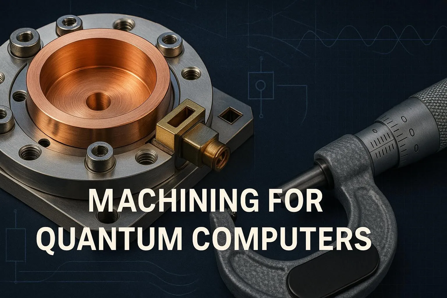
Typical Parts We Machine for Quantum Hardware
- Superconducting qubit packages & cavity halves (
OFHCcopper,Al 6061-T6, occasionallyNb; often soft-gold plated, indium-gasketed) - Cold-finger thermal interfaces & heat spreaders (
OFHC Cu, Ag or Au flashed, lapped) - UHV chambers, adapter plates, and CF flanges (
316L/304L,OFHC Cugaskets) - Ion trap and photonics mounts, alignment stages, and kinematic bases (
Al 6061,Ti,Cualloys;PEEK/Vespelinsulators) - Microwave connector fixtures, waveguide adapters, and shielding enclosures (Al/Cu with precise coax alignment; SMPM/SMA footprints)
The Numbers That Matter (and Why)
Below are typical request ranges we see in quantum projects. They’re not universal specs—your design may need tighter or looser numbers—but they’re practical starting points.
1) Geometry & Fit
- Positional tolerances (dowel pins, coax footprints, optical bores):
±5–20 µm (±0.0002–0.0008")
Why it matters: Keeps microwave launch geometry and optical axes where the simulation assumed. - Flatness of mating planes (package halves, thermal interfaces):
≤5–10 µm over 50–100 mm spans
Why it matters: Prevents seam gaps (microwave loss) and boosts thermal contact area. - Parallelism & perpendicularity (RF cavities, kinematic mounts):
≤10–20 µm over full stack height
Why it matters: Keeps modes and optical paths from drifting; preserves preload distribution.
2) Surface Roughness (Ra)
- Microwave cavities & package interiors:
≤0.4 µm Ra (16 µin); high-Q or gold-plated parts often target ≤0.2 µm (8 µin) or lapped.
Why it matters: Smoother surfaces reduce conductor loss and seam resistance. - Thermal interfaces to cold stages:
≤0.2 µm Ra (8 µin); lapped faces common; pair with indium foil or soft gold for low contact resistance.
Why it matters: Better finish = lower thermal boundary resistance. - UHV sealing (CF knife-edge regions, gasket lands):
16–32 µin Ra and absolutely burr-free.
Why it matters: Ensures reliable metal-to-metal seals and minimizes leak paths.
3) Materials & Treatments
- OFHC Copper (C101/C110, high purity): Thermal pathways, cavities; sometimes soft gold plating for corrosion resistance and lower seam resistance.
- Aluminum 6061-T6: Stable, machinable; often used for enclosures and mounts; can be gold-plated for RF/thermal.
- Stainless 316L/304L: UHV structures; frequently electropolished and vacuum-cleaned.
- Titanium (e.g., Grade 2/5): Low mass, lower thermal contraction than Al/Cu; useful for optical/fixture components.
- Polymers (PEEK, Vespel SP-1): Cryo-compatible insulators with low outgassing.
Cryogenic contraction reality check: Al and Cu shrink ~0.3–0.4% from room temp to 4 K; Ti shrinks far less (~0.08–0.1%). Design allowances and stack-up analysis are essential so cold assemblies tighten rather than open.
What Goes Wrong When Precision Slips
- Shorter coherence times: Poor seams/finishes create extra microwave loss; modes shift; parasitics appear.
- Thermal bottlenecks: Warped or rough thermal joints raise contact resistance; devices don’t fully thermalize.
- Vacuum headaches: Burrs and smeared copper trap oils; rough surfaces outgas longer; seals weep.
- Alignment drift: Angular/position errors compound across stages; rework in the cryostat is slow and expensive.
Ziqual’s Approach: Consistency, Precision, Speed
Quantum builders need parts that work first install, not after three rounds of “tap-and-try.” Ziqual is set up for that outcome.
Process Control & DFM
- Front-end DFM pass specific to cryo/UHV/RF: fillets vs. sharp corners, seam paths, dowel strategies, CTE allowances.
- Material-aware toolpaths: Copper gets high-sharpness inserts, controlled chip load to prevent smearing; micro-endmills for fine features; wire EDM where corners must be truly sharp.
Finishing & Cleanliness
- Rough → semi-finish → finish strategies that preserve geometry.
- Lapping / diamond fly-cut options for mirror-like faces on thermal/RF surfaces.
- Electropolish & passivation (stainless), soft gold (RF/thermal), indium interfaces (where specified).
- UHV-friendly cleaning: aqueous/alkaline wash, ultrasonic DI, solvent rinse; lint-free handling; optional vacuum bake; hydrocarbon-controlled packaging.
Metrology That Matches the Ask
- CMM for true position, flatness, and parallelism at the single-micron level.
- Optical profilometry/confocal for Ra verification down to sub-micron—and for spotting smeared copper that contact stylus might miss.
- Microscope deburr & seam inspection on all UHV/RF faces.
- DNA – Digital Nameplate Archive: Every part’s “recipe” (tools, toolpaths, metrology, finishes, plating lots, cleaning steps) is QR-linked to the part. Reorders repeat exactly—across shops and runs.
Throughput Without Compromising Tolerances
- We stage jobs so tight-tolerance faces are cut last (temperature-stable windows, fresh tooling).
- “Madness Mode” (when you’re in a hurry) still respects finish and metrology gates; no skipping the steps that protect coherence times.
Quick Spec Guide (Copy/Paste Into Your Drawing Notes)
- Mating plane flatness: ≤5–10 µm over 50–100 mm
- Parallelism (package halves): ≤10–20 µm
- True position (dowel/coax/optic): ±5–20 µm
- Interior finish, RF cavities: ≤0.4 µm Ra (16 µin); target ≤0.2 µm (8 µin) for high-Q or lap + plate
- Thermal interface finish: ≤0.2 µm Ra (8 µin) and specify lapped; use indium or soft Au where allowed
- UHV sealing regions: 16–32 µin Ra, burr-free, no media-blast on knife-edges
- Cleanliness: UHV compatible; no silicone oils; specify ultrasonic + solvent + bake if needed
- Plating: Soft gold on selected RF/thermal faces; call out thickness & masking
- Marking: Laser on non-sealing surfaces only; avoid residues on RF paths
- Cryo allowance: Note CTE strategy (fits tighten cold; avoid trapped stress)
(If you send us your current prints, we’ll translate these into a one-page “quantum machining callout” sheet for your program.)
Tolerance-to-Physics: A Handy Mental Map
- +10 µm gap at a seam → higher seam resistance → lower Q, possible mode splitting.
- +0.2 µm Ra on a thermal face → higher Kapitza/contact resistance → warmer device, elevated quasiparticles.
- +0.1° angular error across an optical/ion stage → alignment drift, lower coupling efficiency.
- Burr at CF edge → microscopic leak path → vacuum degradation, more collisions, more heating.
How to Work With Ziqual on Quantum Parts
- Share context, not just a STEP file. Tell us the cold stage, target $T$, RF frequency band, and what’s mission-critical (Q, thermalization time, pump-down time, etc.).
- Co-spec finishes. We’ll recommend where to lap, where to gold-plate, and where “good machining” is enough.
- Lock the recipe with DNA. Your approved run gets archived: tools, feeds/speeds, inspection plan, cleaning, plating lot numbers—the works. Reorders behave identically.
- Scale without drift. If we move your work across partner shops, the same recipe and same gages go with it.
Closing Thought
In quantum, “pretty close” is often “not close enough.” The upside: with the right callouts and a disciplined machining + metrology pipeline, the hardware becomes boring—in the best way possible. That’s how you keep your scientist time on experiments, not rework.
Want us to sanity-check your drawing or convert it to a quantum-ready spec sheet? Send it over—we’ll mark it up and propose a manufacturable, testable recipe.